Testing Transistor DC Gain (hFE) in My Lab
hFE stands for “Hybrid parameter forward current gain, common emitter”, and is a measure of the DC current gain of a bipolar junction transistor (BJT).
The hFE concept is central to transistor usage since it is a measure of small current amplification. There are several hybrid parameters within the transistor hybrid model, including hFE. The hybrid parameters model has fallen out of popularity, so β or beta is now the most common symbol for DC current gain. I will continue to use hFE in this article since datasheets continue to use this name as well.
The hFE parameter value on the other hand is a bit querulous. Many “how-to” articles and DIY circuits describe how to measure hFE based on the simple notion that hFE = IC/IB. Yet, transistor datasheets offer a range of values for hFE under various collector current (IC) conditions. Manufacturer test conditions also use a pulse test (<= 300 uS) where the transistor is active for about 2% of the time (duty cycle). Continuous current tends to cause temperature buildup within the test device. So IC and IB are dynamic entities that may not correlate accurately with static testing. Meanwhile the hFE value for any individual device – even with the same part number and manufacturer – will be different. All combined, attempting to use a specific hFE value for a particular device is a querulous event and can be avoided.
Table of Contents
- Why I measure hFE
- PEAK Atlas DCA Pro – Semiconductor Analyzer
- hFE Socket On Some Digital Multimeters
- Fluke Multimeter
- Measure hFE Using an Oscilloscope and Arbitrary Waveform Generator (AWG)
- hFE Testing Summary
- References
Why I measure hFE
Many engineers tell me that in their 20+ years of design, they have never needed to know a device’s hFE value. Many designs use an estimated hFE of 100, then create a bias network around the transistor to handle a wide range of devices each with different hFE values from 50 to 250 for example, and under different temperatures.
A circuit that depends on a particular value for beta is a bad circuit.
Paul Horowitz, Winfield Hill “The Art of Electronics”
In my experimenter’s role, I want to know my device’s hFE. I have found that each transistor part I own in my “junk box” and even new parts I order from various sources such as Digi-Key, Newark, eBay, and Amazon can be tested for DC gain before use even if my measured value is not a true hFE. So long as the test procedure is repeatable it can be used to verify transistor gain, grade unknown transistors, and match paired devices for use in such applications as push-pull amplifiers, temperature compensation, or current mirrors for example. Transistors treated poorly can also affect the device’s hFE. In fact, during my tests in this article, I discovered an astonishing issue with respect to one device under test. See “Figure 20: Figure 20: Oscilloscope / AWG function generator results” now to see what I mean.
What follows is a tail of hFE tests for two transistor devices from my parts bin: an NPN 2N3904 and a PNP 2N3906…
PEAK Atlas DCA Pro – Semiconductor Analyzer
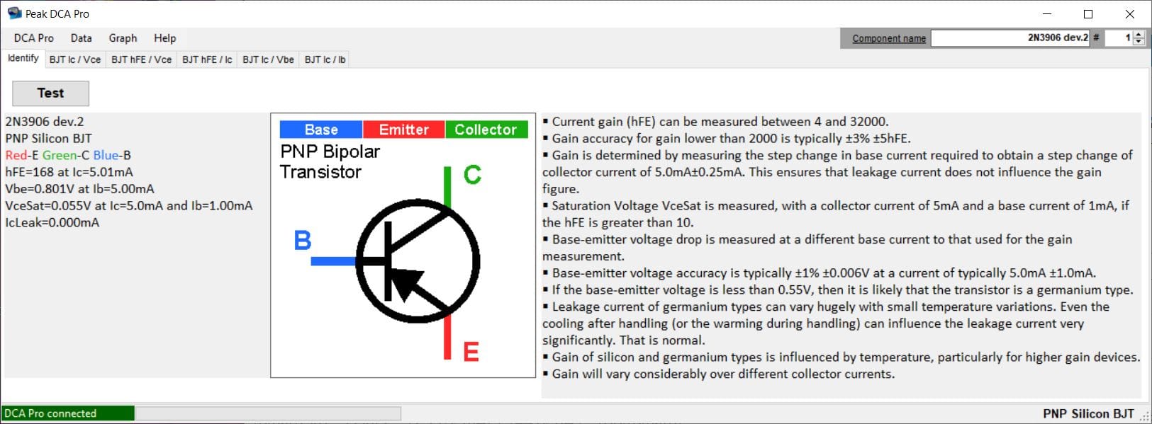
For about $150 (USD) this instrument with a PC interface is my best resource for measuring hFE and many other transistor parameters. A little pricy but it does a great job. Device testing includes small-signal devices, power transistors, FETs, MOSFETs, Diodes, and more. The hFE value is corrected for collector-emitter leakage (useful for germanium transistors).
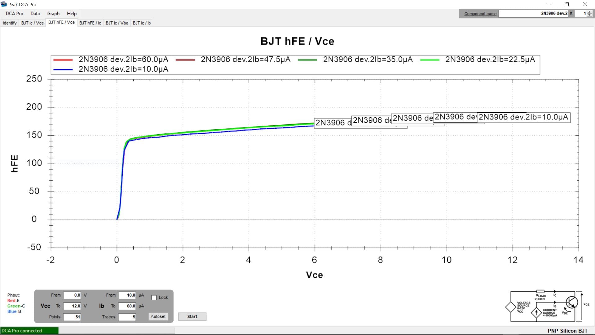
In figures 2 and 3 below, the hFE curves demonstrate how it is affected by base current IB and VCE . In particular, the 10 uA base current hFE curve for the 2N3906 may indicate additional problems as shown later in this article. Here the hFE is significantly lower compared to higher base currents.


Figure 2: 2N3904 DCA Pro results (click image to enlarge).

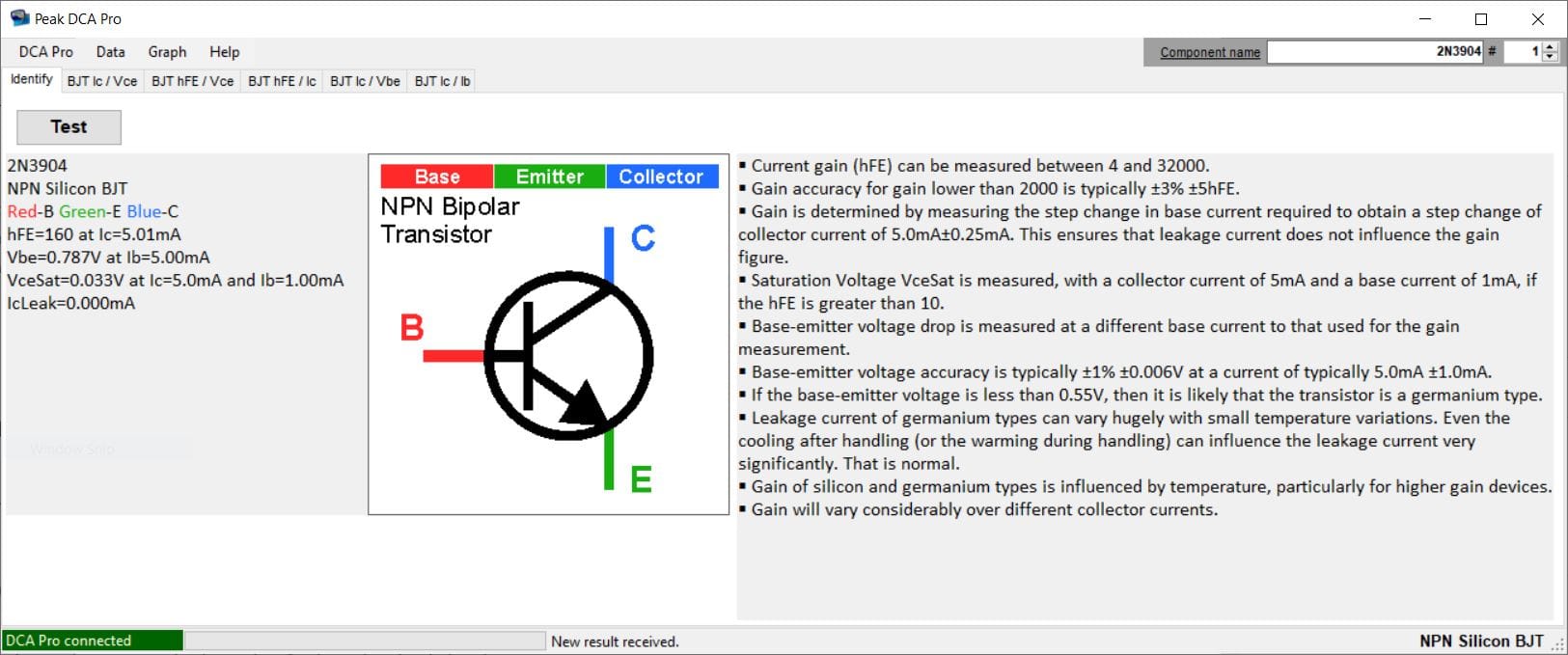

Figure 3: 2N3906 DCA Pro results (click image to enlarge).
hFE Socket On Some Digital Multimeters
This socket will provide a DC gain value useful for small signal silicon device sorting and testing. The socket will not be accurate for germanium transistors as they are usually associated with collector-emitter leakage. It won’t be useful for power transistors either that require more base test current (IB). Some meters with an hFE feature describe the test conditions while others offer no support for their device under test conditions.
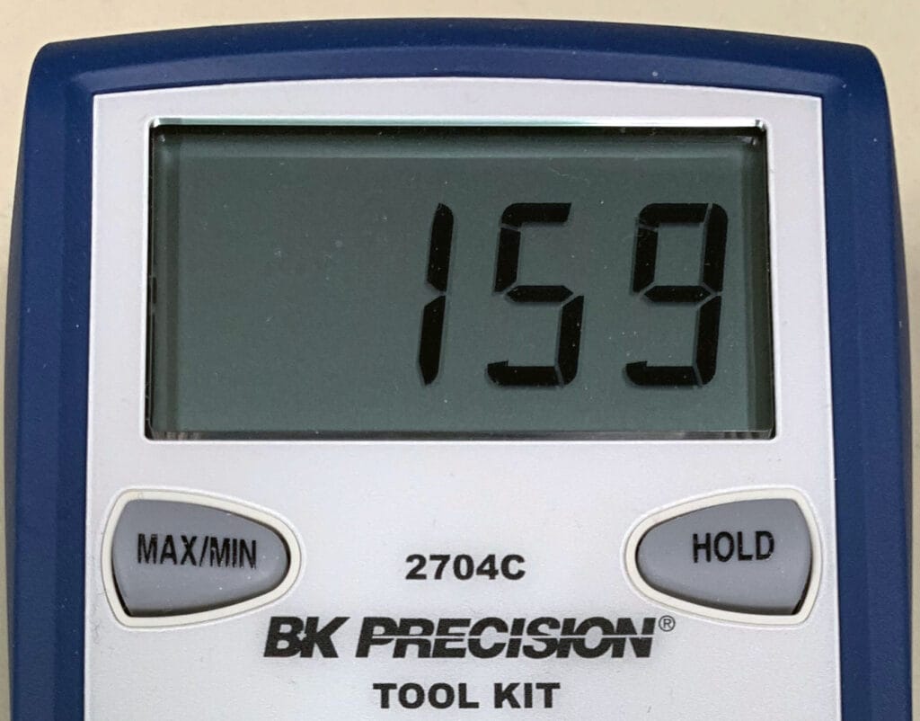
My BK 2704C multimeter does document the hFE socket test conditions:
Range: 0 ~ 1000
Base current: 10uAdc approx. (VCE = 3.0Vdc)
The 2N3906 device I am using for this article (B&K image below right) with a base current of 10 uA predicts a much lower hFE compared to higher base currents as shown in 2N3906 results using the DCA Pro above (Figure 3). While the hFE for the 2N3904 (B&K image below left) is consistent with the DCA Pro results for 2N3904 above since the 10 uA test condition is grouped with the other IB curves. But for sorting and comparing devices, the 10 uA test condition limitation may be just fine.

Figure 4: B&K 2704C multimeter hFE DC current gain measurement for 2N3904 left and 2N3906 right.
Fluke Multimeter
My Fluke meters don’t have an hFE socket. Most other high-end DMMs don’t have an hFE socket either. Some folks say this is because the multimeter reading is not too close to the official hFE reading, others say that the circuit and socket to measure hFE invalidates safety considerations. A great discussion can be found here:
Topic: How come the transistor beta hFE test is only on cheap DMMs?
The diode test feature on my Fluke meters measures semiconductor forward voltage drop under constant current conditions suitable for identifying PNP vs NPN, and which pin is associated with the emitter, base, and collector. But does not offer a way to measure DC current gain.
What follows are some breadboard circuits I use to measure hFE with my DMM…
Test 1: Two Resistors on a Breadboard with hFE Calculation from DMM Results
DC current gain can be calculated by measuring the voltage drop across a base resistor and the corresponding voltage drop across a collector resistor. The schematic for a PNP device is shown in the LTSpice diagram below – Figure 5: “Simulation of Simple 2-Resistor DMM hFE Measurement”. Reverse the polarity of V1 to test NPN devices. Math calculations make this test method a little tedious for sorting a bin of transistors but it is a good substitute for Fluke’s missing hFE socket.
| The figure to the right shows my LtSpice simulation of a simple breadboard circuit for the 2N3906 PNP transistor. This circuit will work with any small signal silicon PNP device. To use NPN devices reverse the polarity of V1. The simulation file can be downloaded from the link found at end of this article. | 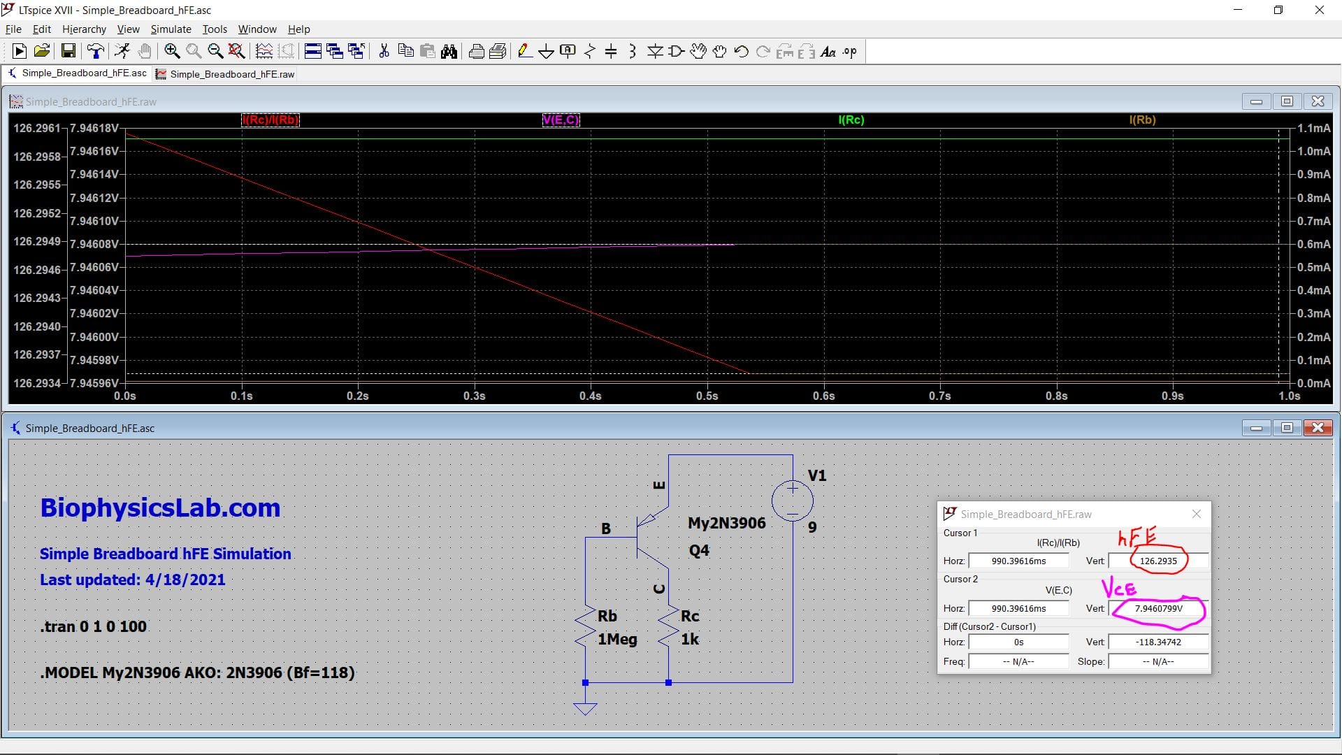 Figure 5: Simulation of Simple 2-Resistor DMM hFE Measurement. |
The breadboard is shown below with PNP 2N3906 (same as the LTSpice schematic and simulation above). I show the hFE calculations for the same two-transistor parts tested with the BK multimeter and DCA Pro above for comparison.
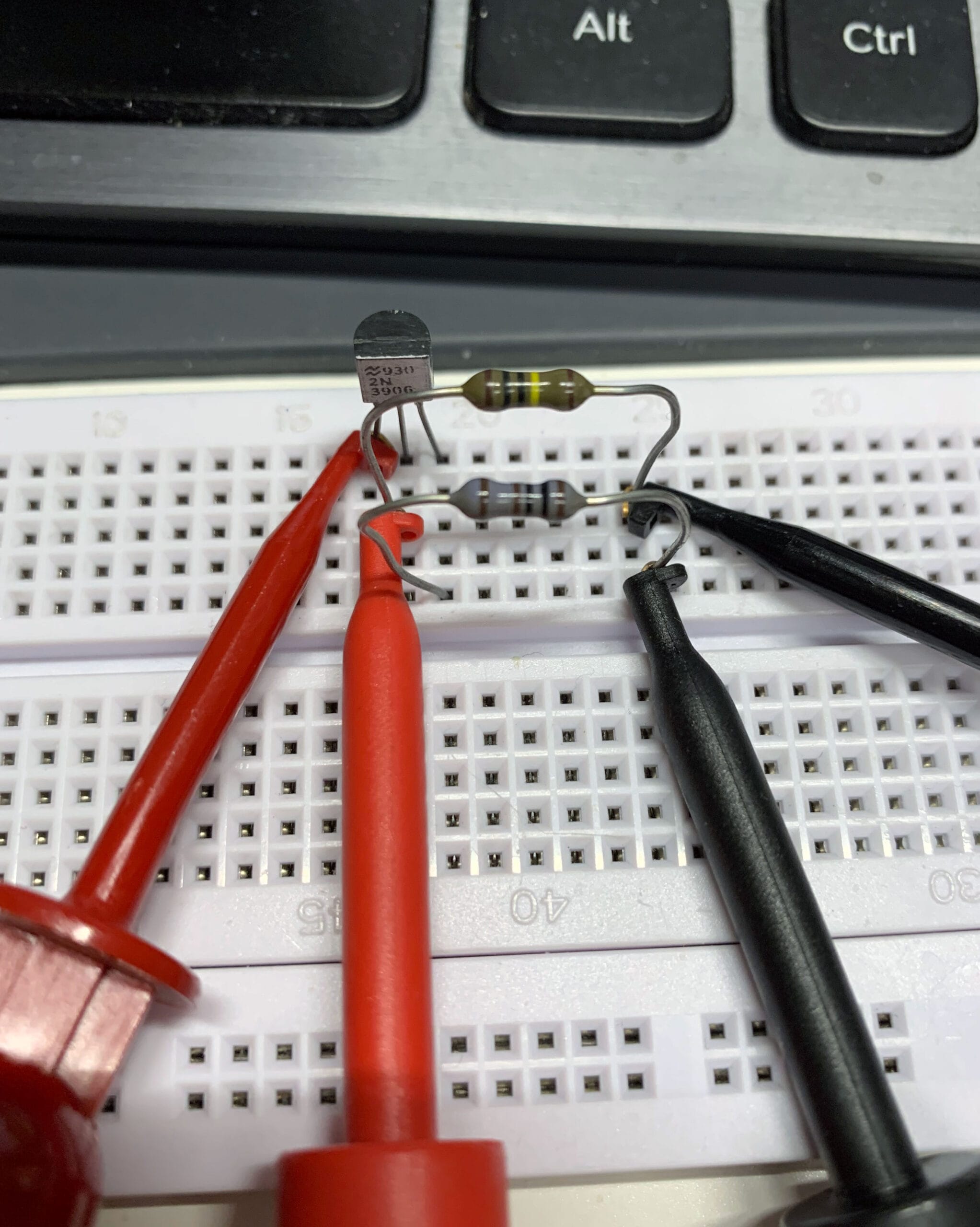
| Device: 2N3906 PNP Power Supply Setup: Vcc = 9.001V, 0.872 mA Measurements: Vce = 8.232V Rb = 0.9969M (1M) Rc = 1.0064k (1k) Vrb = 8.338V Vrc = 0.7646V Calculations: Ib = 8.34V/1M = 8.338 uA Ic = .765V/1k = 765 uA hFE = 765/8.34 = 92 | Device: 2N3904 NPN Power Supply Setup: Vcc = 9.001V, 1.368 mA Measurements: Vce = 7.647V Rb = 0.9969M (1M) Rc = 1.0064k (1k) Vrb = 8.327V Vrc = 1.3508V Calculations: Ib = 8.33V/1M = 8.33 uA Ic = 1.351V/1k = 1351 uA hFE = 1351/8.33 = 162 |
Test 2: Constant Current Source with DMM Direct hFE Readout
By using a few more parts I was able to improve my breadboard testing for use with my Fluke DMM. This version from Circuits Today includes support for both PNP and NPN devices and provides a constant IB current of 10 uA and direct reading of hFE (mA x 100). One problem I noticed: If I put the wrong type of transistor into a socket (swapping NPN for PNP by mistake for example) the transistor under test gets very hot.
KiCad’s Eeschema schematic. See the reference section below for the download file.
Before building this circuit I used LTSpice to simulate.
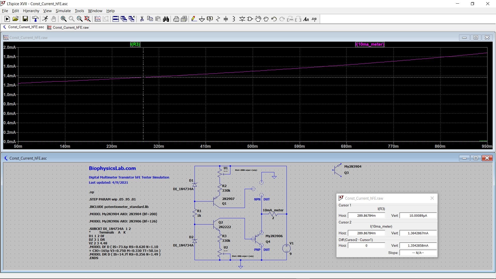
The simulation shown above has potentiometers with simulated wiper arms. The potentiometer library was supplied by Helmut Sennewald – founder of the LTSpice user group. The trace shows the wiper arm going from .05% to 95% with an anticipated calibration for 10 uA at the 29% position for current passing through Q1’s emitter. The simulation file with the potentiometer library can be downloaded from the link found at end of this article.
Final breadboard circuit with 2N3906 device under test…
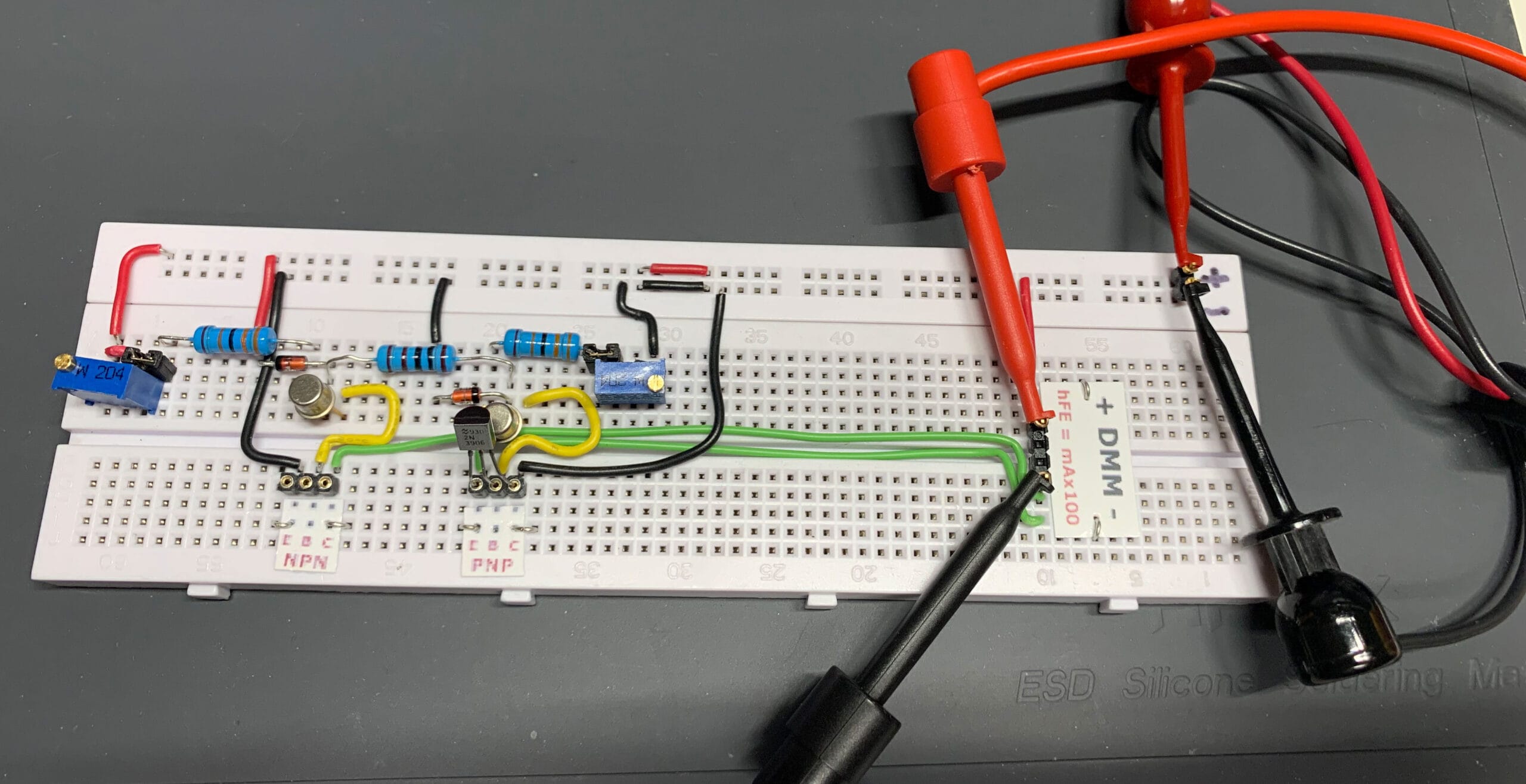
The breadboard circuit shows jumpers next to each pot. These can be opened up one by one with the DMM current meter pins shorted for 10 uA calibration of both the PNP and NPN base to emitter current.


Figure 10: 2N3906 results using the constant current breadboard.


Figure 11: 2N3904 results using the constant current breadboard. Note: Current draw for NPN 2N3904 is much higher than that used by the 2N3906 – consistent with larger hFE.
Measure hFE Using an Oscilloscope and Arbitrary Waveform Generator (AWG)
This method allows for a higher current applied to the transistor under test than either test methods 1 or 2. By using a staircase waveform applied to the transistor’s base and variable voltage applied to the transistor’s collector the temperature of the device under test does not rise enough to affect the stability of the readings.
Simulate the NPN transistor test circuit in LTSpice…
Here are the Piecewise Linear (PWL) text files that control voltage for staircase and triangle waveforms. See the reference section at the end of this article to download files for the full simulation.
pwl_triangle.txt
0		0
+4.17m	10
+4.17m	0
pwl_stair.txt
0s		0.7
8.33m	0.7
8.34m	1.4
16.66m	1.4
16.67m	2.1
24.99m	2.1
25.00m	2.8
33.32m	2.8
33.33m	3.5
41.65m	3.5
41.66m	4.2
49.98m	4.2
49.99m	4.9
58.31m	4.9
58.32m	5.6
66.64m	5.6
66.65m	0.7
Steps to build the simulation (see text and asc file in the reference section of this blog post):
- Apply triangle wave with a frequency of 120 Hz, 10 VP-P, and DC Offset 5 V to transistor under test collector. Simulate the arbitrary waveform generator using the LTSpice Piecewise Linear Function (PWL) using data points in a text file. See attached file: pwl_triangle.txt.
- Create a staircase wave with a frequency of 15 Hz, 5 VP-P, and a DC Offset of 0.7 V (start wave at an amplitude above VBE to turn on the transistor under test). Again with PWL and a text file of data points. See attached file: pwl_stair.txt.
- Layout parts for a simulation of the simple breadboard circuit.
- Define a 1-second transient analysis to kickstart LTSpice simulation.
- Simulate a scope using passive probes with the common ground (no differential probes used).
- Plot X-axis as VCE using Ch2.
- Plot first Y-axis as Ic using a math function: (Ch1-Ch2)/100.
- Plot the second Y-axis as IB using a math function: (Ch3-Ch4)/100000.
Calculate simulated 2N3904 NPN transistor hFE as IC/IB at selected VCE. See “Figure 12: LTSpice simulation of oscilloscope / arbitrary waveform generator NPN transistor hFE test circuit” above for details. For example: At VCE of 5 V and 4th IB curve (representing IB = 27.7 uA).

Simulate the PNP transistor test circuit in LTSpice…
The PNP circuit is the same as the NPN transistor test circuit. Only the polarity of the staircase and triangle wave functions have been reversed. The staircase wave now goes from -700 mV to -5 V. The triangle wave now goes from 0 V to -5 V.
Here are the Piecewise Linear (PWL) text files that control voltage for staircase and triangle waveforms. See the reference section at the end of this article to download the full simulation.
pwl_triangle_minus.txt
0		0
+4.17m	-10
+4.17m	0
pwl_stair_minus.txt
0s		-0.7
8.33m	-0.7
8.34m	-1.4
16.66m	-1.4
16.67m	-2.1
24.99m	-2.1
25.00m	-2.8
33.32m	-2.8
33.33m	-3.5
41.65m	-3.5
41.66m	-4.2
49.98m	-4.2
49.99m	-4.9
58.31m	-4.9
58.32m	-5.6
66.64m	-5.6
66.65m	-0.7
Calculate simulated 2N3906 PNP transistor hFE as IC/IB at selected VCE. See “Figure 13: LTSpice simulation of oscilloscope / arbitrary waveform generator PNP transistor hFE test circuit” above for circuit details. For example: At VCE of 5 V and 4th IB curve (representing IB = -28.0 uA).

Final breadboard circuit with 2N3904 NPN transistor under test…
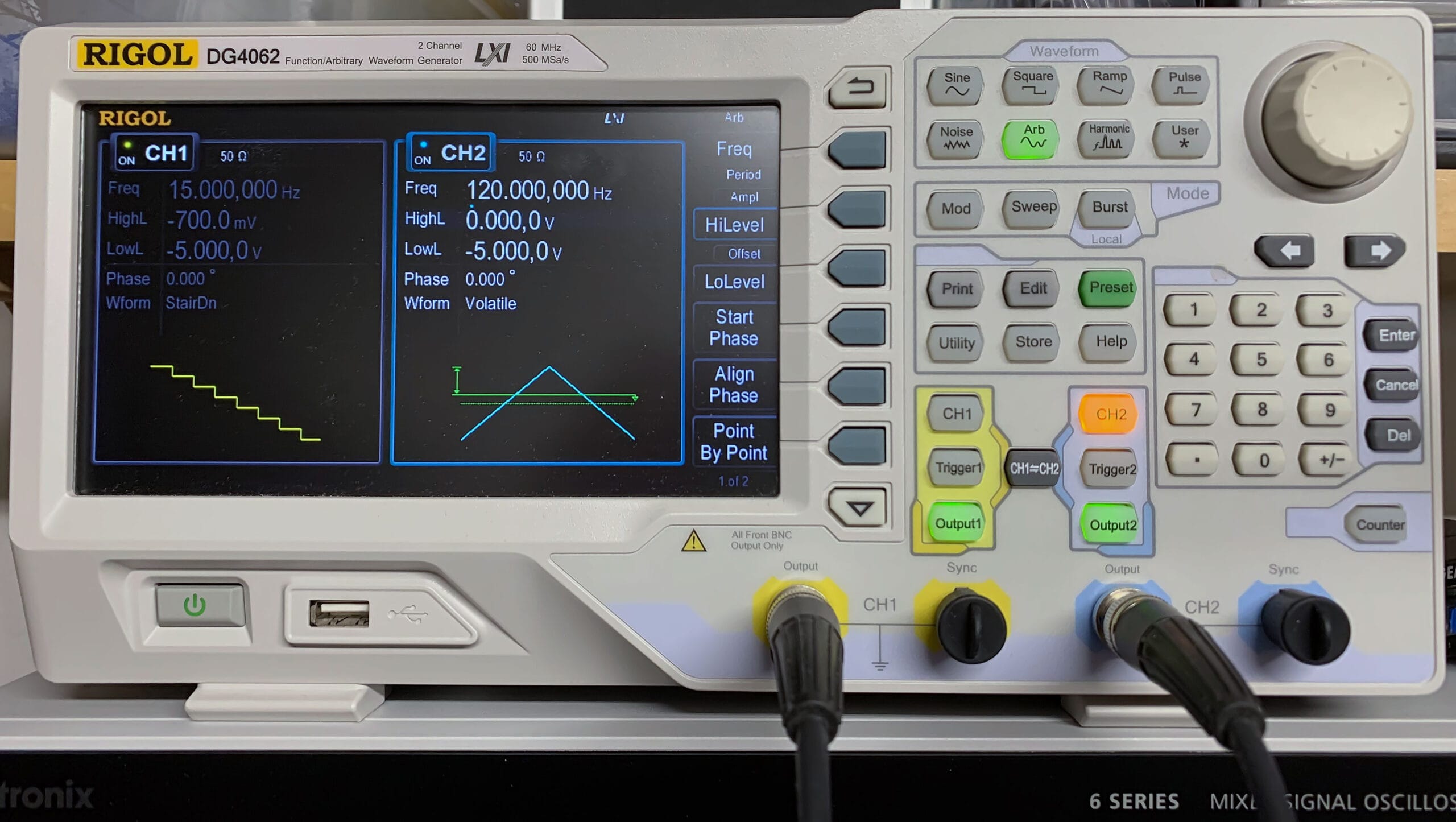
I used a two-channel arbitrary waveform generator to create transistor base and collector signals:
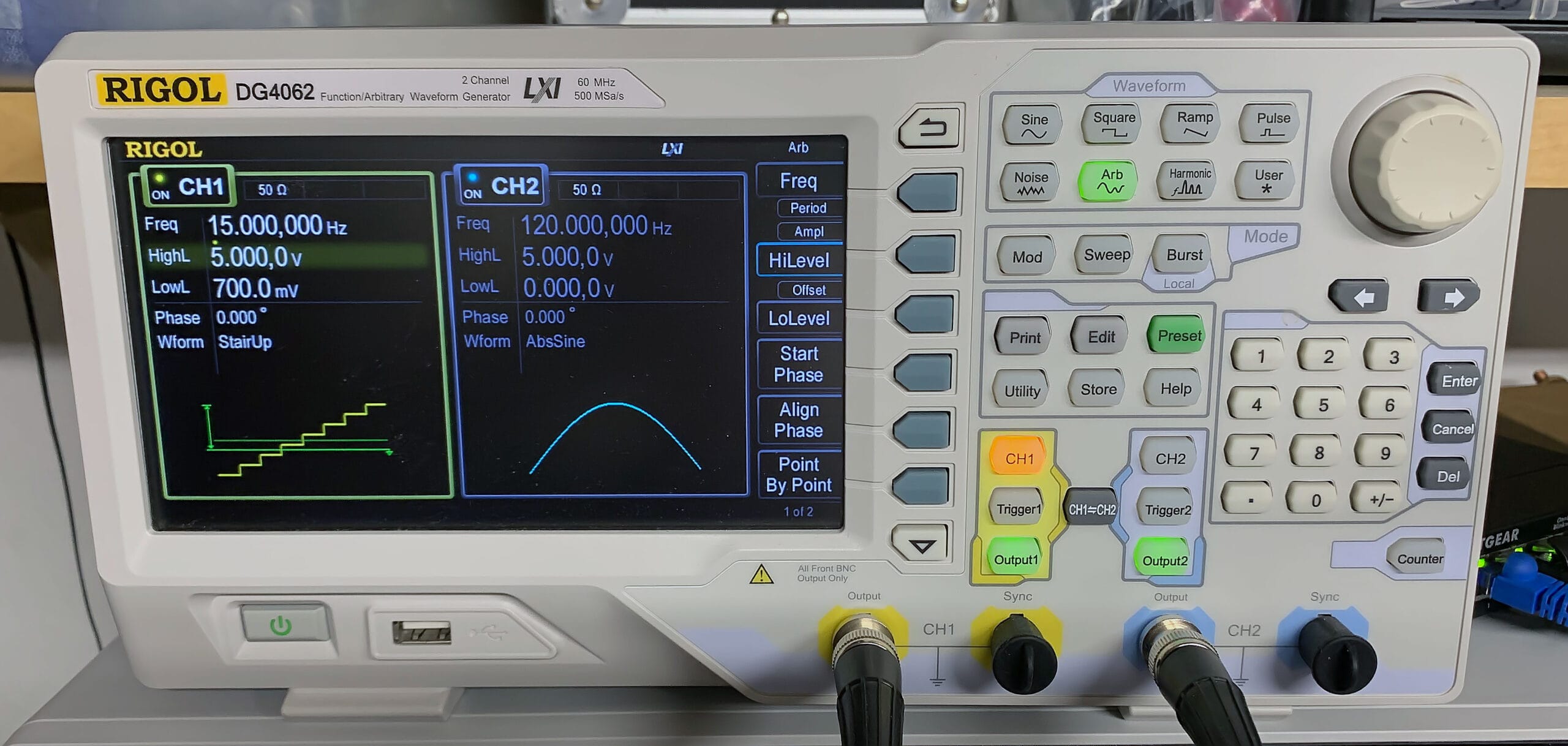
- Channel 1 uses StairUp (staircase with 8 levels) arbitrary waveform with a frequency of 15 Hz, a high level of 5 V, a low level of .7 V, and a phase of 0.
- Channel 2 uses an AbsSine arbitrary waveform with a frequency of 120 Hz, a high level of 5 V, a low level of 0 V, and a phase of 0. Note: an AC step-down transformer with a full-wave rectifier circuit would produce the same waveform for those with only one channel AWB.
- Use the align phase option on the Rigol DG4062 AWB so channel 2 produces exactly one cycle for every staircase level of channel 1. See Figure 16 below for an example with cursors.
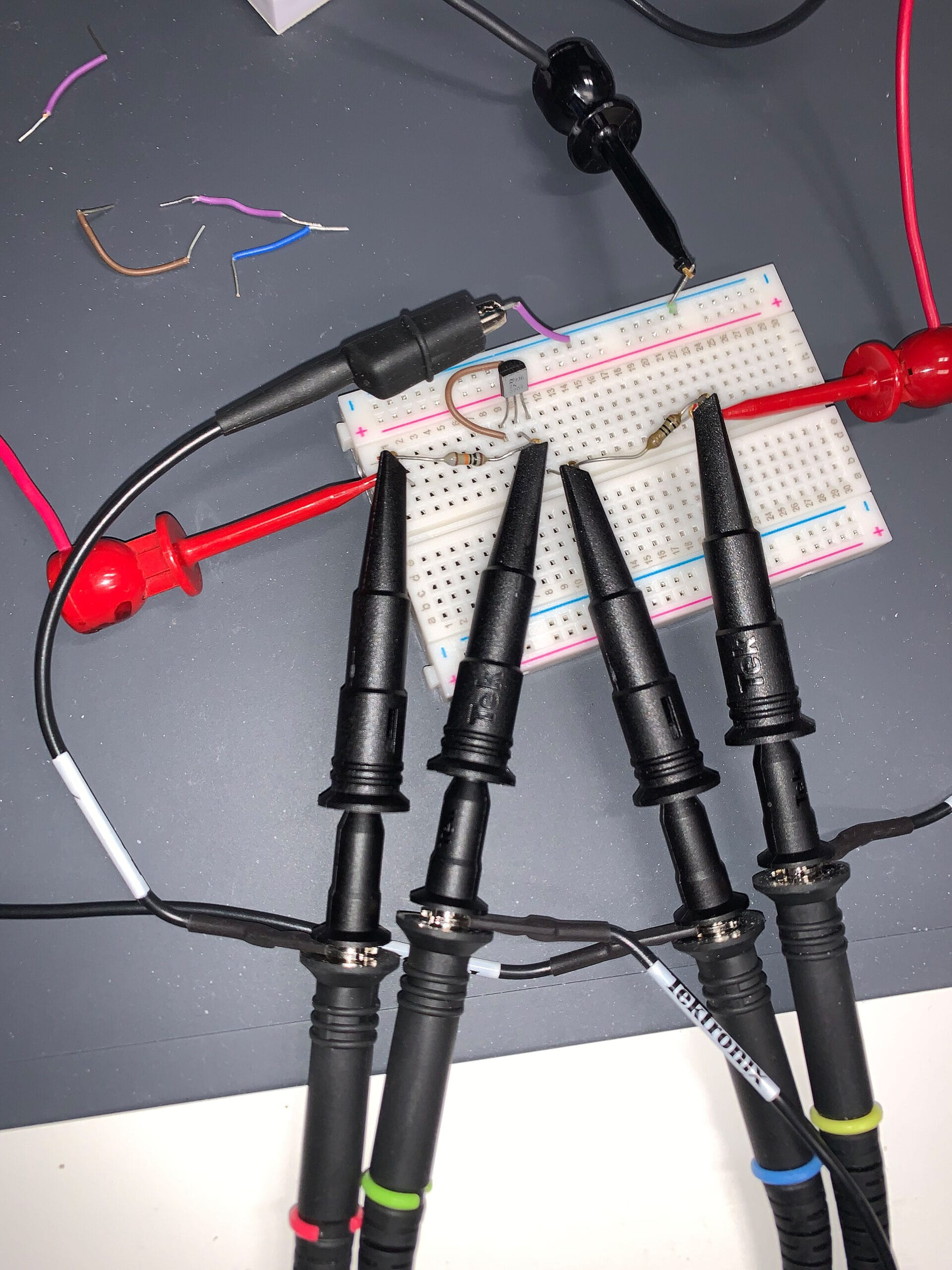
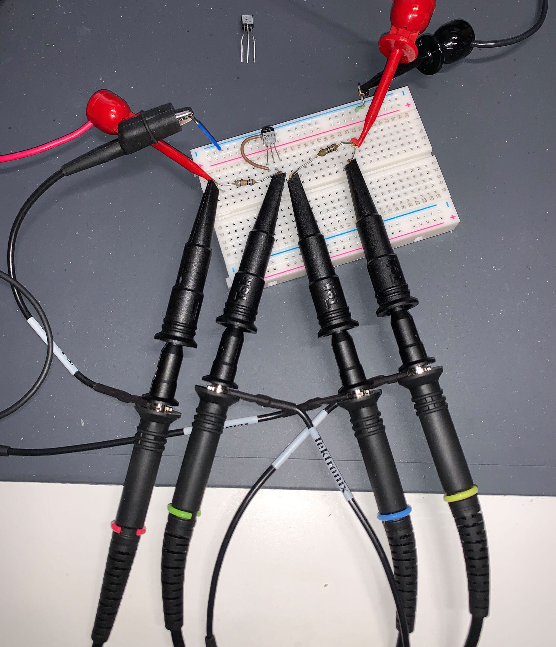
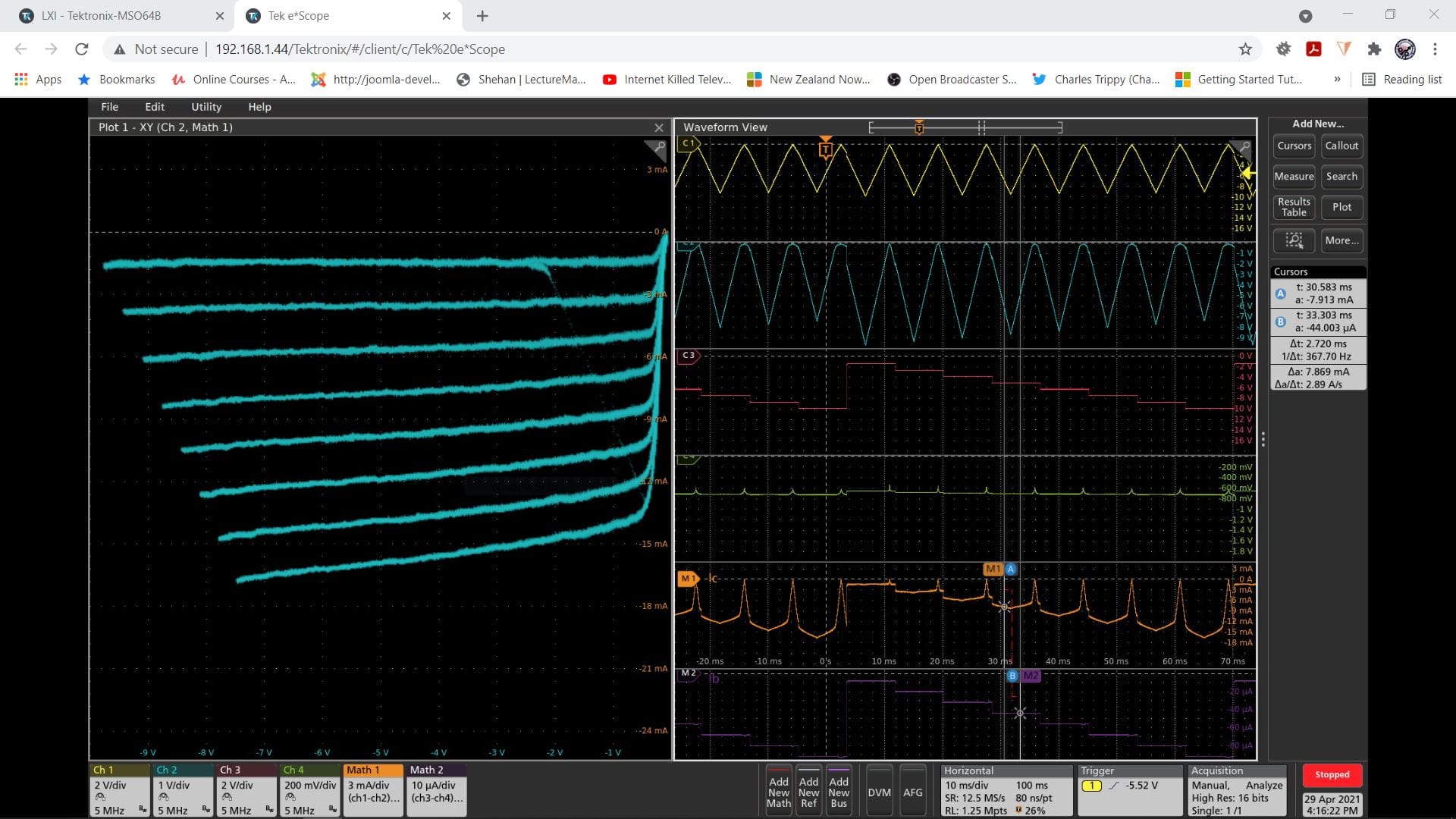
Build the simple NPN 2N3904 transistor two-resistor breadboard with 4 scope channels connected. See Figure 12 above for the schematic and Figure 15 below for the breadboard layout.
- Connect 100kΩ resistor between 2N3904 transistor base and AWG channel 1. Connect scope probes Ch3 (green) and Ch4 (red) across this resistor to measure base current IB.
- Connect 100Ω resistor between 2N3904 transistor collector and AWG channel 2. Connect scope probes Ch1 (yellow) and Ch3 (blue) across this resistor to measure collector current IC and VCE.
- Connect transistor emitter to ground. Tie AWG and scope to the ground as well.
Oscilloscope Setup, see Figures 16 and 17 below…
- Ch 1 = 2 V/div, 20 MHz Bandwidth -> Clip to resistor “+” side of Rc in Figure 12
- Ch 2 = 2 V/div, 20 MHz Bandwidth -> Clip to resistor “-” side of Rc in Figure 12 -> Represents transistor under test Vce
- Ch 3 = 1 V/div, 20 MHz Bandwidth -> Clip to resistor “+” side of Rb in Figure 12
- Ch 4 = 100 mV/div, 20 MHz Bandwidth -> Clip to “-” side of resistor Rb in Figure 12
- Math 1 = 2 mA/div, (Ch1-Ch2)/100, Alternate units A -> Represents transistor under test Ic
- Math 2 = 5.4 uA/div, (Ch3-Ch4)/100000, Alternate units A -> Represents transistor under test Ib
- Horizontal = 10mv/div, 12.5 MS/s, 1.25 Mpts
- Trigger = Edge, Ch 1, DC coupling, Level 2.64 V, Rising edge
- Acquisition = High Res, Stop after 1 acquisition, Internal time source
- Set up XY Plot with transistor VCE (Ch 1) for X and transistor IC (Math 1) for Y
- Set up a linked waveform cursor to measure IC (Math 1) and IB (Math 2) for hFE calculation
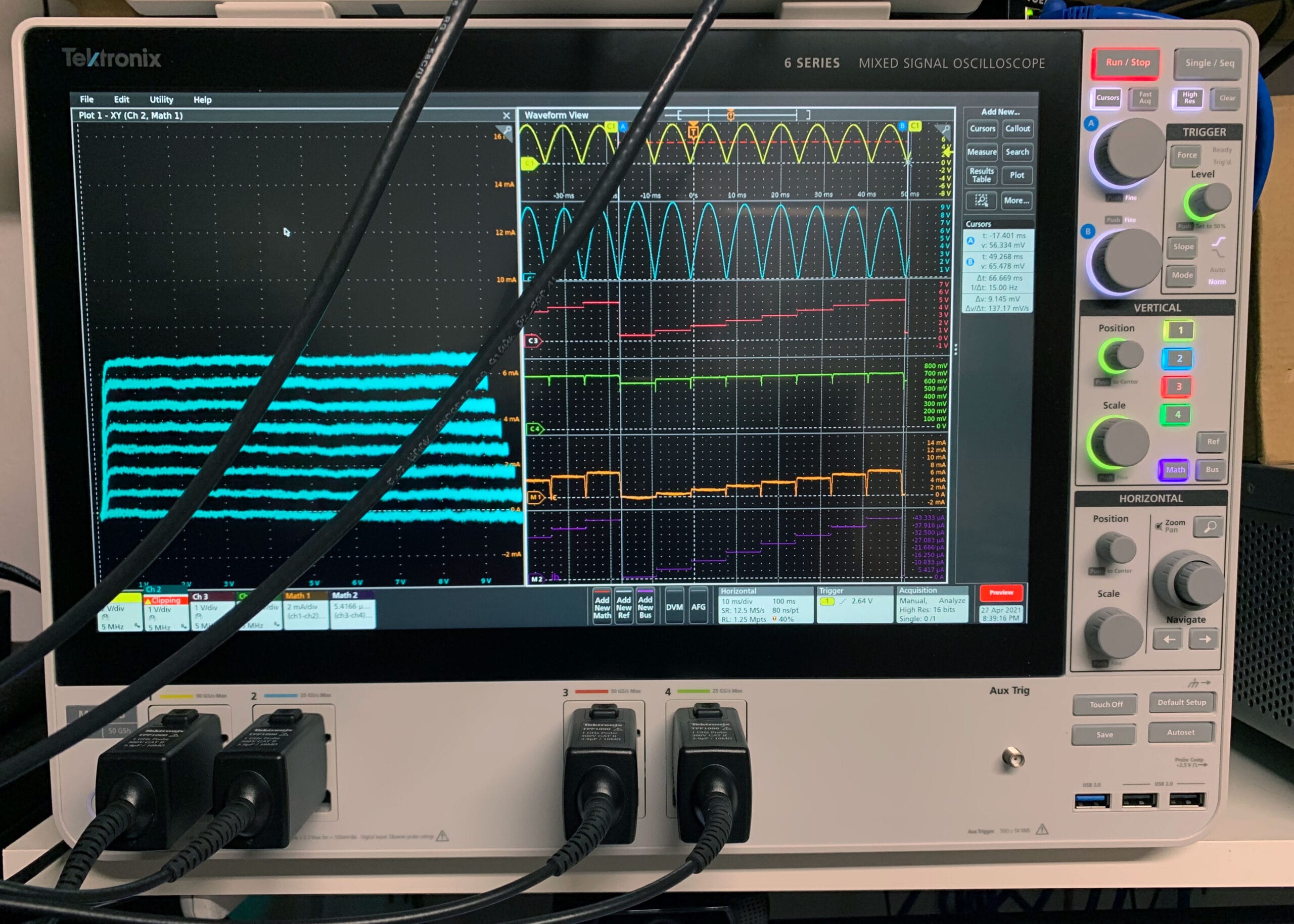
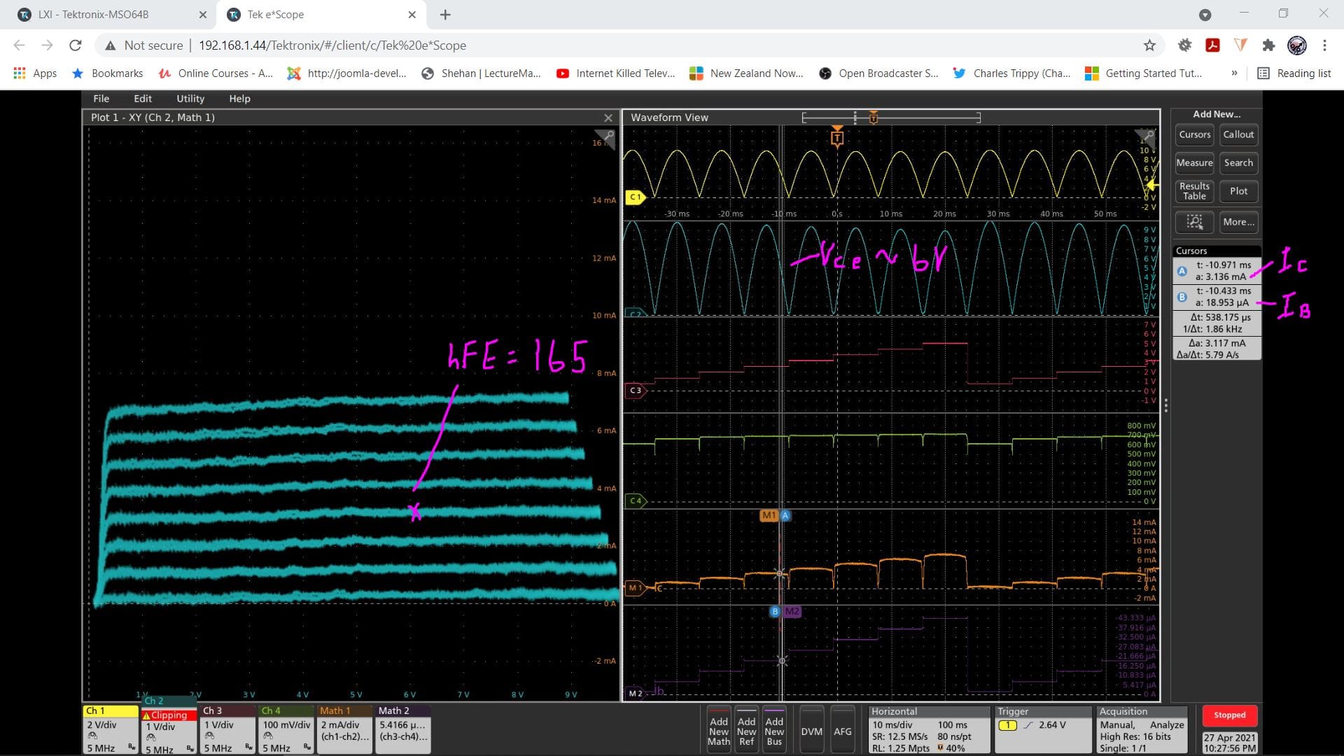
Calculate 2N3904 NPN transistor hFE as IC/IB at selected VCE. For example: At VCE of 6 V and 4th IB curve (representing IB = 18.95 uA).

The hFE of 165 measured from the scope is the same value shown in Figure 2: 2N3904 DCA Pro results.
Final breadboard circuit with 2N3906 NPN transistor under test…
Reuse the same circuit as shown in Figure 13 above for the schematic. Change the AWG function generator signals to go negative. I also switched the collector signal from AbsSine to Triangle. A negative AbsSine waveform did not produce as clear a result as the Triangle waveform. Perhaps I could have inverted the AbsSine wave from the Rigol utility menu first but did not try. See Figure 18 below for settings.
Breadboard…
Oscilloscope results…
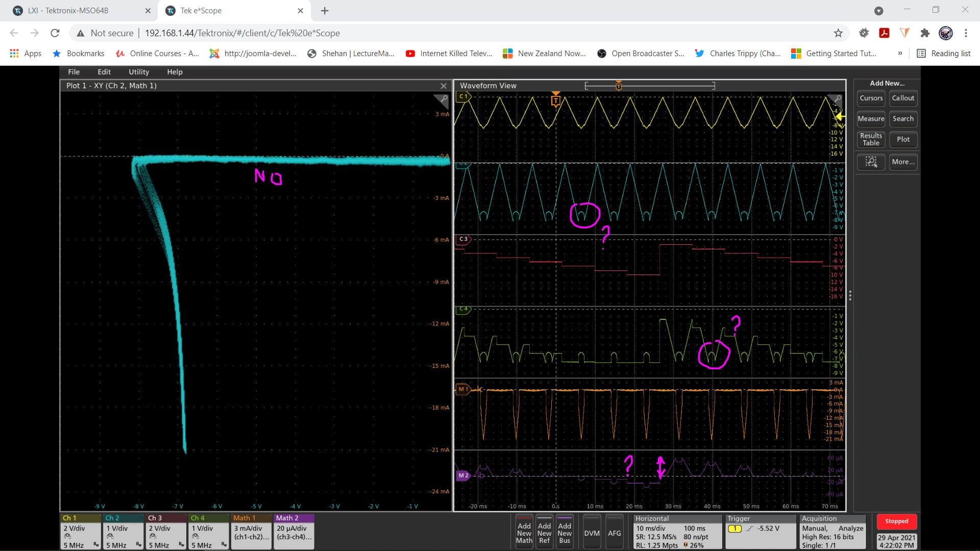
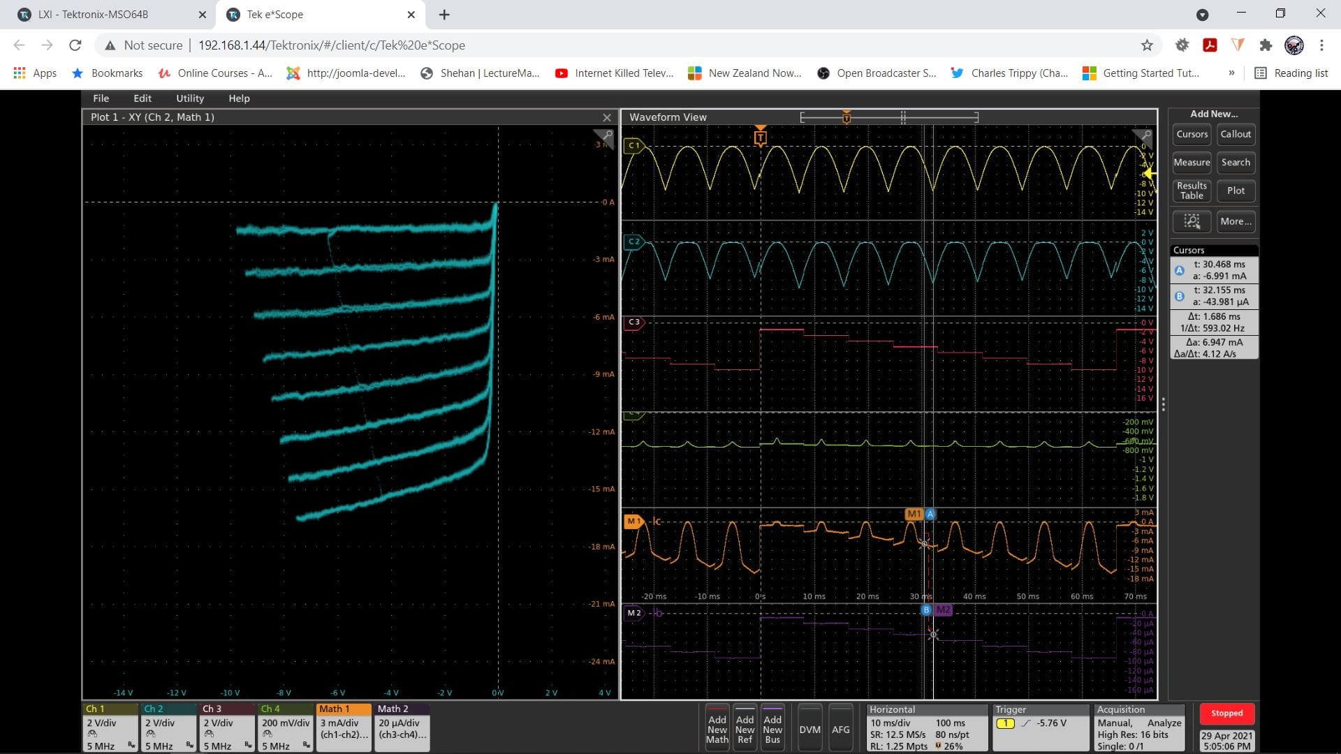
Unfortunately, my first 2N3906 PNP device failed during this test – See Figure 20 (left). DCA Pro hFE and curves still look the same. But under this scope/AWG test, the device beaks down when VCE is greater than about 7 V. Several other PNP transistors were tested including other 2N3906 devices. These other devices tested just fine. One user on Electronics Stack Exchange had the following comment that seems right to me:
Looks like the CE junction got zapped and acts as a SCR with a negative incremental resistance . Might be good for a tunnel diode oscillator at RF if biased at -7V. 😉 This is a breakdown arc failure with say 40K/mm might be 40V/um so 7V is about a 175 nm gap that the E-Field bridged This PNP should be good to -40V and act like a Zener near -50V. In the 70’s I needed a HV Zener for uA ref. So I choose a transistor breakdown voltage to make the old TV work.
Tony Stewart EE75
Reading from the A and B cursors from Figure 20 image on the right: IC [Math 1: (Ch1-Ch2)/100] = 7.913 mA and IB [(Ch3 – Ch4)/100,000] = 44.0 uA at selected VCE of 6 V.

Unfortunately, I did not set the A and B cursors very accurately for VCE of 6 V so the hFE value is not as accurate as it could have been. But the efficacy of this test method is still relevant.
See below for a comparison to hFE using the PEAK DCA Pro semiconductor analyzer for my new PNP 2N3906 that I call device 2.
hFE reading for PNP 2N3906 Dev2 using BK 2704C hFE socket. Low VCE and low IB are the cause for consistently lower readings from multimeter hFE sockets. Yet the testing is very easy, quick, and comparable from one transistor to the next for sorting and matching purposes. But some device under-test issues can not be seen with this simple test.
Figure 22: 2N3906 transistor under test using hFE socket on BK 2704C multimeter.
hFE Testing Summary
Each test method presented here is useful under some conditions. For most testing purposes, the DMM Diode setting would be sufficient.
But using an oscilloscope and AWG function generator allows for very meaningful transistor exploration including hFE.
References
| hFE LTSpice Simulations | ||
|---|---|---|
| Two Resistors on a Breadboard | Zip File | |
| Constant Current Breadboard | Zip File | |
| Oscilloscope / Arbitrary Waveform Generator Breadboard | Zip File |
| KiCad | ||
|---|---|---|
| Constant Current Source with DMM Direct hFE Readout Schematic | Zip File |
| Bibliography | ||
|---|---|---|
| Semiconductor Device Measurements by John Mulvey, Tektronix, 1st Ed, 1969 | Web Link | |
| How come the transistor beta hFE test is only on cheap DMMs? | Web Link | |
| Constant Current hFE Transistor Tester | Web Link | |
| Semiconductor Curve Tracer With the Analog Discovery 2, Instructables, brmarcum, 2016 | Web Link | |
| Using an Arbitrary Waveform Generator & Digital Storage Oscilloscope to Create a Transistor Curve Tracer, Circuit Specialists, George Leger, 2014 | Web Link | |
| Modeling Bipolar Junction Transistors – YouTube – ElectronX Lab | YouTube Link (start at 112s for h-Parameters) |
At 70, I decided to tackle EE vai Kahn Academy/USN NEETS and Art of Electronics. I was a HS VocEd in the late 60s and went on to get my Ph.D. in Policy Analysis. I just set up my learning lab with some Fluke 8084s, a Sig SDS 1204Ex. I also got hold of a BK 501A curve tracer. In the early 70s, who THOUGHT about measuring nanoVolts and nanoAmps? Fortran/Python/Cobal Compilers online? Remarkable.
Anyway, your explanations and descriptions are very clear. I posted this article on EEVBLOG/Beginners. It should encourage users on that forum to build your setup and learn.
Thank you for this.
Thank you Dewey. I love EEVBLOG.
Thank you for the excellent document .
Warm South Africa greetings.
Jan v d Linde
Communica Pty Ltd
Samrand
Centurion
SA